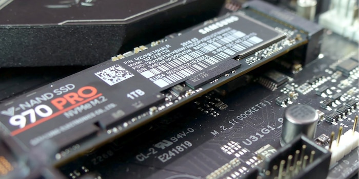
SSD operation is a complex business
SSDs are increasingly replacing hard disks as the main form of mass storage. Their speed and mobility offer undeniable advantages. Data is read and written electrically, not mechanically. How do they work?
Every year sees the emergence of a new generation of processors that are more than promising. The average user doesn't really notice, but the same can't be said for SSDs. The switch from HDD to SSD is noticeable, regardless of how it's used.
I used to turn on my computer and go and get a coffee while it booted up.... I fell head over heels in front of a notebook with an SSD drive. It was like going from a regional train to a TGV. Or from walking to running. Anyway, you get the idea.
But what makes SSD drives so fast? Unlike hard drives, they don't have read heads, write heads or rotating platters. Each block can be accessed at the same speed. It doesn't matter whether they're next to each other or on another module. So there's no point in defragmenting them. Access times are shorter, and read and write speeds are higher.
So I've decided to dedicate an article to it. Once you understand how these discs work, their wear and tear will make sense. And you'll also be able to clear up some previously unanswered frequently asked questions. Why SSDs slow down when they run out of storage space, for example.
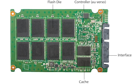
A word of warning before we dive into the heart of the matter: some passages are highly technical. A solid state drive consists of a board with an interface (SATA, PCIe, SATA-Express or other), NAND flash memory, cache memory depending on the drive, and a controller on which the firmware is located. It is controlled via a protocol (AHCI or NVMe). Let's start with NAND flash memory.
What is NAND flash memory
In contrast to hard disks, data is electronically read from and written to NAND flash memory. This is distinguished by its high storage capacity and good data protection. It does what platters do on a hard disk: it backs up data permanently by creating a voltage.
Bit lines and word lines
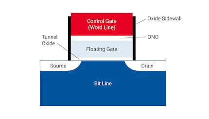
A NAND block consists of bit lines and word lines. The bit lines are parallel. They are made of silicon and are separated by a technique called "shallow trench isolation" (STI). The word lines, made of polysilicon, are perpendicular to the bit lines. The control gate is placed on these lines. The memory cell is located where the bit line and word line intersect.
The individual memory cells are so-called Floating Gate Metal Oxide Semiconductor Field Effect Transistors (FGMOS). The floating gate is located between the control gate and the bit line. It is an electrically insulated semiconductor layer that stores charge and floats in the insulation layer. The electrons in the floating gate do not discharge for two to ten years, even when not energised.
Let's take a closer look at the interface between the bit line and the word line, along the word line to be precise. The control grid surrounds the floating grid. The two grids are separated by an oxide-nitride-oxide (ONO) layer. Below the floating gate is the tunnel oxide (non-conductive), then the bit line with the source and drain.
Pages, blocks, planes and "dies"
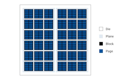
The memory cells in a word line are grouped together in a page. Pages are the smallest units that can be read from or written to an SSD. Depending on the manufacturing process or the type of flash memory, pages can be 2KB, 4KB, 8KB or 16KB.
Several pages are grouped together in blocks. Each block comprises between 128 and 256 pages. A block is the smallest unit that can be erased. Technically, erasure could also take place at page level, but the voltage required would be so intense for the memory cells that the lifespan would be further shortened. I provide more information on the use of memory cells below.
The blocks, meanwhile, are generally spread over two planes per flash module (also known as "dies"). The modules come to rest on the board. There they are connected to the controller via four to ten channels.
Small aside: the slowdown of SSDs
How data is read and stored
To simplify, data in a flash memory is recorded when electrons are placed on or removed from the floating gate. The bits are read using the voltage. When electrons are present on the floating gate, the bit has a value of 0. When none are present, the bit has a value of 1. Memory cells are considered empty or erased when they have a value of 1 and written when they have a value of 0.
.
Let's take a closer look at this and start with reading.
Reading
Erasing
Writing and programming
When writing, electrons are transferred to the floating gate, and a bit value of 0 is obtained. When a high positive voltage is applied to the control gate and another is simultaneously applied to the drain, electrons can pass through the oxide layer and reach the floating gate. This process is called hot electron injection.
SLC, MLC and TLC memories
The SLC memory
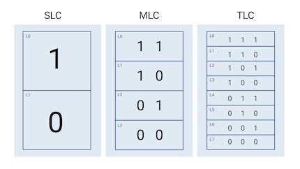
Since only one bit is stored per memory cell, the failure rate is very low. Only two voltage levels are required for reading and writing, which increases speed and reduces power consumption. SLC flash memories are considered to have a lifetime of 100,000 write cycles per block.
MLC memory
TLC memory
TLC flash memory differs more clearly from SLC and MLC memory. It costs even less to manufacture than MLC. Memory cells have to withstand eight voltage levels. Reading takes around four times as long, and writing six times as long as with SLC memory. We're talking about a lifetime of 1,000 write cycles per block.
Another little aside: the lifespan of an SSD drive
As I've already mentioned, writing data is only possible to an empty or erased memory cell. Overwriting data itself is impossible. Data must first be erased and then rewritten to be modified. The lifetime of an SSD drive is therefore measured in write cycles.
The controllers and the processor
Write amplification
Garbage collection
Garbage collection is a background process used to counter SSD slowdowns as memory capacity decreases. Partial blocks are copied and assembled into new, complete blocks. The old blocks are then erased, freeing them up for rewriting. This does not limit accesses to the SSD.
The TRIM
Wear management (wear leveling)
The future
The other methods of increasing memory in a limited space have been mentioned in the paragraphs devoted to MLC and TLC memories. But there is a physical limitation here too. To finish my article, I'd like to look again at two approaches that have increased the memory capacity and speed of SSDs and will continue to do so in the future.
3D NAND or V-NAND memory
The NVMe protocol
From big data to big brother, Cyborgs to Sci-Fi. All aspects of technology and society fascinate me.
Interesting facts about products, behind-the-scenes looks at manufacturers and deep-dives on interesting people.
Show all